在这里记录自己的嵌入式学习方向和成果,只做大方向的规划,目前学习规划如下:
√ linux基础学习
√ arm裸机开发(使用正点原子IMX6ULL的板子)
√ linux的系统移植
√ Linux核心驱动开发
√ qt
√ linuxc应用编程
【doing】linux内核源码分析(主要通过以下两本书并结合linux源码进行学习):
- linux内核设计与实现(在看)
- 深入理解linux内核
在现代多核处理器系统中,处理器核心的组织方式和任务分配策略直接影响系统的软件设计与通信方式。按照核心间的共享程度,多核系统通常可以分为 对称多处理(SMP, Symmetric Multi-Processing) 和 非对称多处理(AMP, Asymmetric Multi-Processing) 两类。
SMP 系统中的所有核心平等地共享同一份内存和 I/O 资源。每个核心运行相同的操作系统实例,一个核通过_start初始化以后,唤醒其他的核做secondary_start_kernel,可以执行任意任务,并通过统一的调度器协调任务执行。
AMP 系统中,各个核心独立运行自己的操作系统实例或裸机程序,它们之间可能不共享内存,甚至运行不同类型的操作系统。典型应用包括 异构多核 SoC,如 Cortex-A 与 Cortex-M 核组合,或者 CPU 与 DSP 的混合系统。
特性 | SMP | AMP |
---|---|---|
核心对等性 | 所有核心对等 | 核心独立 |
操作系统 | 单实例,多核心共享 | 每核心独立操作系统 |
内存访问 | 全部共享 | 部分共享或不共享 |
通信方式 | 共享内存 + IPI 中断 | 消息通道(RPMsg / Mailbox) |
通信目标 | 任务同步、调度、资源管理 | 命令下发、事件通知、数据传输 |
调度应用
场景:当一个 CPU 修改了任务优先级 / 唤醒了一个任务,但该任务更适合在另一个 CPU 上执行时。
做法:当前 CPU 向目标 CPU 发送 IPI,目标 CPU 立即触发调度器,切换到这个任务
跨核函数调用(smp_call_function)
场景:某个内核子系统需要在所有 CPU 上执行一段代码,比如linux下的fiq-debugger机制:当某个核卡死的时候依然可以通过smp_call_function让该卡死的核执行传入的回调函数,在调试的时候非常好用,比如我的代码导致了某一个核卡死了,可以通过smp_call_function的机制让卡死的核dump一些信息
做法:一个 CPU 发 IPI 给其他 CPU,让它们都执行一个回调函数。
核间通知 / 快速消息传递
在linux下多个a核间的通讯相对来说比较简单,主要是通过向需要通讯的核发一个ipi中断来实现,ipi中断以及中断处理函数在初始化的时候进行注册
IPI 的全称是 Inter-Processor Interrupt,中文一般叫 处理器间中断 或 核间中断。
它的作用就是在 **多核处理器 ** 系统里,让一个 CPU 主动“打断”另一个 CPU,从而实现 跨核通信与协作。
先看一些定义: linux内核支持的ipi调用
1 | enum ipi_msg_type { |
为每个核注册ipi中断(也就是gic控制器的SGI中断–注册为软件中断):
1 | void __init set_smp_ipi_range(int ipi_base, int n) |
看一下ipi的处理函数
1 | //看一下都支持哪些中断处理 |
这里拿IPI_CALL_FUNC来举例,场景是我们需要唤醒某个cpu执行一个函数(比如dump当前的reg):ps – 为了方便理解整体的链路,代码部分我进行了一定的删减,因此与实际上的linux的代码有差异,感兴趣可移步至源码kernel/smp.c与arch/arm/kernel/smp.c中阅读
处理部分主要分为两个链路,一个是发ipi的链路,一个是处理ipi的链路,先看发ipi中断的链路:
1 | //这里其实就是处理所有发送ipi中断请求的接口,属于芯片架构层(这里会调用不同中断处理器的架构注册的回调函数) |
既然中断已经发送过去了就需要看一下对应的中断处理函数,也就是generic_smp_call_function_interrupt:代码依旧只保留了关键逻辑
1 | static void flush_smp_call_function_queue(bool warn_cpu_offline) |
我们可以写一段测试程序来验证一下我们上面所说的框架:
1 | #include <linux/module.h> |
这里只是做了一行打印,但是我们在回调函数中的自由度是非常高的,所以可以做一些非常有意思的事情,例如dump当前cpu的一些信息
所以总的来说,linux下的smp间的通信就是基于下发ipi中断来实现的,整体的流程也非常的简单:
初始化阶段
内核启动时,会调用 set_smp_ipi_range()
为 每个 CPU 注册好所有支持的 IPI 中断号(SGI → 对应 ipi_handler
)
所有 IPI 的入口统一落到 ipi_handler()
→ do_handle_IPI(ipinr)
通信阶段
某个 CPU 需要和别的 CPU 通讯时 → 调用 smp_cross_call(cpumask, ipi_nr)
本质就是往目标 CPU 发一个 IPI 中断(SGI)
处理阶段
目标 CPU 收到 IPI → 进入统一的 ipi_handler()
根据 IPI 类型 分发到不同的处理逻辑:
IPI_CALL_FUNC
→ 执行 generic_smp_call_function_interrupt()
,在目标 CPU 上调用函数IPI_RESCHEDULE
→ 执行 scheduler_ipi()
→ 触发一次 schedule()
调度IPI_CPU_STOP
→ 停止 CPUIPI_IRQ_WORK
→ 执行 irq_workIPI_CPU_BACKTRACE
→ 打印 backtrace举一反三(线程切换例子)
如果我们想让某个 CPU 立刻执行一次线程切换:
1 | // 发一个 IPI_RESCHEDULE 到目标 CPU -- 可能会封装好api,但是最终都会走到这里 |
在目标 CPU 上最终执行的就是:
1 | case IPI_RESCHEDULE: |
所以完全可以推断:**IPI_RESCHEDULE 的处理函数就是触发 schedule()**。
图示如下:
1 | graph TD |
由于a核和m核心之间通信方式有很多,大部分要看soc内部的硬件实现,比如mailbox,共享内存等等的机制,对于机制的具体实现本节我们不过多关注,但是linux提供了一个rpmsg的框架,用于向用户屏蔽底层差异。源码位于 driver/rpmsg下
rpmsg在linux中作为一个单独的总线实际上和其他类似platform,iic,pcie总线类似,总线的主体都是由probe,remove,match组成的。
先看一下这个结构:
1 | /** |
我们以rockchip的核间通讯的驱动为例:
首先会注册一个platform总线的驱动框架用于管理自己的设备资源:
1 | static const struct of_device_id rockchip_rpmsg_match[] = { |
在probe中会注册一个virtio设备,同时注册mailbox通道,将virtio的rx tx 接口设置为mailbox,我们可以理解mailbox是在virtio的下一层,是实际和硬件交互的层级:
1 | //这是我从probe中提取出来的一部分 |
在a核上我们可以将m核作为一个虚拟设备,使用virtio去管理,所以rgmsg基于virtio注册了一个通用的驱动,位于drivers/rpmsg/virtio_rpmsg_bus.c下:
1 |
|
当我们的soc中需要做m核和a核的通讯的时候,我们需要注册一个rpmsg driver以及一个device,而在上面的rpmsg_probe就会执行device的注册,此时我们再需要注册一个rpmsg的driver就可以让这一套机制运行起来了,由于virtio框架内容比较多,这里不纠结底层的实现了,大致流程可以从如下框图看出:
1 | sequenceDiagram |
分析前先看下面这个函数:
1 | .macro get_phy, reg, symbol |
adrp \reg, \symbol
计算symbol相较于pc寄存器的页基地址,可以看成:
1 | reg = (symbol & ~(0xFFF)) - (pc & ~(0xFFF)) + (pc & ~(0xFFF)) |
再通过add \reg, \reg, #:lo12:\symbol将symbol的低12位与reg相加存放回reg中
这么使用是为了解除直接使用ldr reg,=symbol
的限制
首先从内核的入口_start进行分析:
1 | /* Variable registers: x21~x28 */ |
mov dtb_paddr, x0
将设备树的物理地址从x0中取出(由uboot放入x0中)放入dtb_paddr中,由dtb_paddr .req x21
可知dtb_paddr 是寄存器x21的别名,同理,x1-x3中的值会被放入x23-x24中。get_phy stack_top, .boot_cpu_stack_top
将CPU得栈顶地址保存在X25中mov x0, dtb_paddr
将设备树的物理地址放入x0寄存器我们进入init_mmu_early中查看:
1 | init_mmu_early: |
首先获得了early_page_array的物理地址,通过源码可知,early_page_array是预留出来的一片24*4096的地址空间:
1 | .early_page_array: |
再通过 bl set_free_page
将这个地址存入全局变量__init_page_array
中:
1 | void set_free_page(void *page_array) |
将early_tbl0_page
early_tbl1_page
存入x0,x1寄存器中。early_tbl0_page
early_tbl1_page
描述如下:
1 | .early_tbl0_page: |
再通过get_pvoff x2 x3计算物理地址与虚拟地址的差值并存入x3寄存器:
1 | .macro get_pvoff, tmp, out |
该函数先将符号boot_cpu_stack_top的地址(在链接阶段已经确定是虚拟地址)存入tmp寄存器,再将boot_cpu_stack_top的物理地址存入out寄存器,最后相减存回out寄存器
将ARCH_EARLY_MAP_SIZE的值存入x2寄存器
跳转到rt_hw_mem_setup_early
函数,此时x0-3寄存去的值分别为:
将early_tbl0_page和early_tbl1_page映射为2M的页表,分别用于内核态和用户态,而early_tbl0_page
和early_tbl0_page
分别为内核态和用户态l0页表的首地址
再跳转到enable_mmu_early
函数中
enable_mmu_early
:
1 | enable_mmu_early: |
ttbr0_el1
和ttbr1_el1
中kernel_start
的地址返回后由于x30寄存器中存放的是kernel_start
地址所以会跳转到kernel_start
中执行
1 | kernel_start: |
ldr x8, =rtthread_startup
被存放了rtthread_startup
的地址,所以会跳转到rtthread_startup
中执行,接下来就是c的代码的阅读啦~pbuf 结构体:
1 | struct pbuf { |
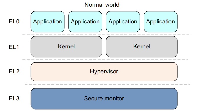
armv8中,执行发生在4个异常级别之一,在aarch64中,异常级别决定了特权级别,类似于armv7中定义的特权级别,异常级别决定特权级别,因此在Eln执行对于特权Pln。类似地,具有比另一个更大的n值的异常级别处于更高的异常级别,一个数字比另一个小的异常级别被描述为处于较低的异常级别。
Linux驱动开发和裸机开发的区别**
Uboot是一个裸机程序,比较复杂,就是一个bootloader。作用就是用于启动Linux或其他系统,Uboot最主要的工作就是初始化DDR(Linux的运行是运行在DDR里面的),一般linux镜像zimage(uimage)+设备树(.dtb)存放在SD,EMMC,NAND,SPI FLASH等等外置存储区域。
Rgb 三原色组成每个像素点,而分辨率就是像素点的个数,而argb则是增加了透明通道,
所以视频视频显示的逻辑是先发vspw开始信号->一段vbp延时(稳定需要?)-> n*(hspw行开始信号->hb屏信号->行像素显示信号->hfp作为到下一行开始信号的延时)->vfp作为到下一帧的信号延时。然后这些信号发送给ser 再通过des解码给屏幕
1 | "vidoeTiming":{ |
串行器连接在外设中,将并行信号转换为串行信号,解串器将串行信号再解析为并行信号
串行解串器的控制是同一个芯片控制还是串行器一个芯片,解串一个芯片,两个分别作为iic的子设备进行控制,主要有几个场景,比如:
时钟数据恢复:将并行的像素数据流与时钟信号合并,并用一种叫做 时钟-数据恢复(CDR) 的机制生成同步的时钟信号,用于后续的串行数据传输。
编码:将并行的数据进行编码转换。通常,为了提高信号的传输效率和抗干扰能力,会使用像 8b/10b 编码 或 10b/12b 编码 等方法。
串行化:将并行的数据进行串行化,TI 935 会把多个并行数据通道(例如 8 位、10 位或 12 位并行数据)按特定的时序顺序串联成一个单一的 串行数据流。这个串行数据流会通过 高速差分信号对(如 FPD-Link 3 协议中的差分对) 进行传输。具体地,TI 935 使用 FPD-Link 3 协议 中的高速串行链路来将这些并行数据转化为串行数据。FPD-Link 3 协议支持非常高的传输速率,能够有效传输 4.5 Gbps 或更高的速率。
数据打包与封装:将编码后的串行数据通过一对或多对 差分信号对 传输到接收端(通常是解串器 TI 960)。FPD-Link 3 使用的差分信号对(如 LVDS 信号对)能够提供高速、低功耗的长距离传输,支持最大 15 米的传输距离(具体距离取决于数据速率和电缆质量)。
时钟恢复与同步:不仅要将数据串行化,还需要通过 时钟数据恢复(CDR) 技术来保持数据和时钟的同步。这是因为,在串行化数据时,时钟信号被嵌入到数据流中,并通过差分信号传输。在接收端(解串器 TI 960)会从串行信号中恢复出时钟信号,并重新同步数据流。
The APB-to-Generic block bridges the APB operations into FIFOs holding the Generic commands. The block interfaces with the following FIFO: Command FIFO, Write payload FIFO, Read payload FIFO.
上面的架构无非就是体现两件事:
Generic interface packets are always transported using one of the DSI transmission modes; Video mode or Command mode. If neither of these mode are selected, the packets are not transmitted through the link and the released FIFOs eventually get overflowed.
通用接口数据包总是使用DSI传输模式之一进行传输;视频模式或命令模式。如果不选择这两种模式,则数据包不会通过链路传输,并且释放的fifo最终会溢出。
The DPI interface follows the MIPI DPI specification with pixel data bus width up to 24 bits. It is used to transmit the information in Video mode in which the transfers from the host processor to the peripheral take the form of a real-time pixel stream. This interface allows sending ShutDown (SD) and ColorMode (CM) commands, which are triggered directly by writing to the register of VO_CON[9:8] in the GRF Module. To transfer additional commands(for example, to initialize the display), use another interface such as APB Slave Generic Interface to complement the DPI interface.
The DPI interface can be configured to increase flexibility and promote correct usage of this interface for several systems. These configuration options are as follows:Polarity control: All the control signals are programmable to change the polarity depending on system requirements.
==After the MIPI DSI HOST Controller reset, DPI waits for the first VSYNC active transition to start signal sampling, including pixel data, and preventing image transmission in the middle of a frame.==
If interface pixel color coding is 18 bits and the 18-bit loosely packed stream is disabled, the number of lines programmed in the pixels per lines configuration is a multiple of four. This means that in this mode, the two LSBs in the configuration are always inferred as zero. The specification states that in this mode, the pixel line size should be a multiple of four.
DPl接口遵循MIPI DPI规范,像素数据总线宽度高达24位。它用于以视频方式传输信息,其中从主机处理器到外设的传输采用实时像素流的形式。该接口允许发送ShutDown (SD)和ColorMode (CM)命令,这些命令通过写入GRF模块中的VO_CON[9:8]寄存器直接触发。要传输额外的命令(例如,初始化显示),可以使用其他接口(如APB Slave Generic interface)来补充DPI接口。可以配置DPI接口以增加灵活性,并促进多个系统正确使用该接口。极性控制:所有的控制信号都是可编程的,可以根据系统设备改变极性。在MIPI DSI主机控制器复位后,DPI等待第一个VSYNC主动转换到一个帧。
==如果接口像素颜色编码为18位,并且禁用了18位松散打包流,则在每行像素配置中编程的行数是4的倍数。这意味着在这种模式下,配置中的两个lsb总是被推断为零。规格规定,在此模式下,像素线尺寸应为4的倍数。==
“The DPI interface follows the MIPI DPI specification with pixel data bus width up to 24 bits.
It is used to transmit the information in Video mode in which the transfers from the host processor to the peripheral take the form of a real-time pixel stream. This interface allows sending ShutDown (SD) and ColorMode (CM) commands, which are triggered directly by writing to the register of VO_CON[9:8] in the GRF Module. To transfer additional commands(for example, to initialize the display), use another interface such as APB Slave Generic Interface to complement the DPI interface.”
总结:
“The DPI interface captures the data and control signals and conveys them to the FIFO interfaces that transmit them to the DSI link. Two different streams of data are presented at the interface; video control signals and pixel data. Depending on the interface color coding, the pixel data is disposed differently throughout the dpipixdata bus. The following table shows the Interface pixel color coding.”
总结:
“If interface pixel color coding is 18 bits and the 18-bit loosely packed stream is disabled, the number of lines programmed in the pixels per lines configuration is a multiple of four. This means that in this mode, the two LSBs in the configuration are always inferred as zero.”
总结:
“These configuration options are as follows: Polarity control: All the control signals are programmable to change the polarity depending on system requirements. After the MIPI DSI HOST Controller reset, DPI waits for the first VSYNC active transition to start signal sampling, including pixel data, and preventing image transmission in the middle of a frame.”
总结:
💡 整体理解:
The MIPI DSI HOST Controller supports the transmission or write and read command mode packets as described in the DSI specification. These packets are built using the APB register access. The GEN_PLD_DATA register has two distinct functions based on the operation. Writing to this register sends the data as payload when sending a Command mode packet. Reading this register returns the payload of a read back operation. The GEN_HDR register contains the Command mode packet header type and header data. Writing to this register triggers the transmission of the packet implying that for a long Command mode packet, the packet’s payload needs to be written in advance in the GEN_PLD_DATA register.
The APB Slave interface allows the transmission of generic information in Command mode, and follows the proprietary register interface. Commands sent through this interface are not constrained to comply with the DCS specification, and can include generic commands described in the DSI specification as manufacturer-specific.
The GEN_PLD_DATA register has two distinct functions based on the operation. Writing to this register sends the data as payload when sending a Command mode packet. Reading this register returns the payload of a read back operation. The GEN_HDR register contains the Command mode packet header type and header data. Writing to this register triggers the transmission of the packet implying that for a long Command mode packet, the packet’s payload needs to be written in advance in the GEN_PLD_DATA register.
总结:
文档列出了很多可通过 Generic Interface 发送的包,包括:
理解:
Generic interface packets are always transported using one of the DSI transmission modes; Video mode or Command mode. If neither of these mode are selected, the packets are not transmitted through the link and the released FIFOs eventually get overflowed.
结论:MODE_CFG 决定控制器整体传输方式,但命令包本身不需要每条切换模式。
The transfer of packets through the APB bus is based on the following conditions:
The APB protocol defines that the write and read procedure takes two clock cycles each to be executed. This means that the maximum input data rate through the APB interfaces is always half the speed of the APB clock.
The DSI link bit rate when using solely APB is equal to (APB clock frequency) *16 Mbps.
To drive the APB interface to achieve high bandwidth Command mode traffic transported by the DSI link, the MIPI DSI HOST Controller should operate in the Command mode only and the APB interface should be the only data source that is currently in use.
The memory write commands require maximum throughput from the APB interface, because they contain the most amount of data conveyed by the DSI link. While writing the packet information, first write the payload of a given packet into the payload FIFO using the GEN_PLD_DATA register. When the payload data is for the command parameters, place the first byte to be transmitted in the least significant byte position of the APB data bus. After writing the payload, write the packet header into the command FIFO.
The DCS long packets are encapsulated in a DSI packet. The DSI included in the diagrams.In the follow figures, the Write Memory Command can be replaced by the DCS command Write Memory Start and Write Memory Continue.
垂直方向(帧级)
在一帧里,垂直方向的时序顺序是:
1 | VSS(Vertical Sync Start / VSA开始) |
水平方向(行级)
每一行的水平时序是:
1 | HSS(Horizontal Sync Start / HSA开始) |
I.MAX6ULL IO初始化流程
缺失模块。
1、请确保node版本大于6.2
2、在博客根目录(注意不是yilia根目录)执行以下命令:
npm i hexo-generator-json-content --save
3、在根目录_config.yml里添加配置:
jsonContent: meta: false pages: false posts: title: true date: true path: true text: false raw: false content: false slug: false updated: false comments: false link: false permalink: false excerpt: false categories: false tags: true